
Scanning Electron Microscope
SEM/EDS Imaging
- Topographic Imaging
- Atomic Number Profile Imaging
- Elemental X-ray Mapping
- Image Segmentation
Imaging Features:
The SEM provides several advantages over light microscopes including greater magnification, greater depth of field, and finer magnification control. Our Scanning Electron Microscope, a JEOL JSM-6360LV, is a digital SEM. It is capable of magnifications of up to 100,000 times in Secondary Imaging mode with 3.0-nm resolution for topographic imaging. The SEM is fitted with a stage that allows for a maximum sample size of 4 inches dia. x 2.5 inches high. It allows for tilting, and rotatation of the sample.

Allowing a small amount of air into the chamber (Low Vacuum mode) neutralizes charges on uncoated, non-conducting materials so that gold coating is not required for plastics, ceramics, and other dielectrics.
Here is an image of a mite found in moss. The image was taken at a magnification of 350x, without any gold sputtering. The head of this little guy measured approximately 50-microns or 0.050 millimeters.
Secondary Electron Imaging
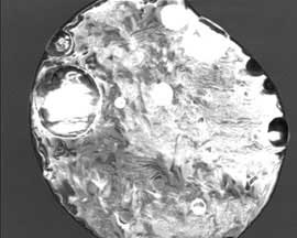
Secondary electron images show the morphology and topography of a sample. The most common form of imaging, Secondary Electron Imaging (SEI) produces a high resolution image of the surface topography of a specimen. In failure analysis, this usually provides enough information to determine the mechanism of failure of a material. The SEM provides several advantages over light microscopes including greater magnification, greater depth of field, and finer magnification control.
Backscattered Imaging
Back scattered electron images show the difference in atomic number over a sample. The higher the atomic numbers of the atom, the brighter the image results for larger atoms. Our SEM allows for three modes of Backscattered Electron imaging. These three modes are available in high or low vacuum modes at 4.0 nm resolution:
- Compo (for Composition): Atomic number contrasting imaging. Lighter elements appear darker while heavier elements appear brighter.
- Topo (for Topography): Surface topography imaging similar to Secondary Electron imaging
- Shadow: Combination of Compo & Topo with illumination from the side.
Secondary Electron Imaging
The secondary electrons are used to create an image of the surface. The angle of the secondary electron projection depends on the angle of the incoming beam. Thus steep surfaces and edges tend to be brighter than flat surfaces, which results in images with a well-defined, 3D appearance, Secondary Electron Imaging.
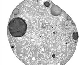
Backscattered Imaging
A backscattered electron profile is also collected as the number of backscattered electrons increases with atomic number, so atoms of a higher atomic number appear brighter in the image. The image is digitally captured with a resolution of down to 5 nm, Backscattered Electron Imaging.
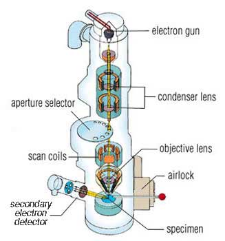
How the SEM works
In the SEM the electrons are emitted from a tungsten filament, and accelerated through a high voltage of 50-100kV . The electron beam is focused by a condenser lense to a spot between 50-100Å in diameter. The beam hits the sample producing backscattered electrons, which are scattered off the surface; secondary electrons, which are emitted from the surface, as they are knocked out of the valence orbitals of the surface atoms, then characteristic X-rays are emitted.
With aid of the sofware, the Secondary Electrons produce topographical imaging, the Backscattered Electrons produce Atomic Number contrast imaging, and the X-rays produced are collected by the edx detector for chemical analysis.
Youtube video of how the SEM works
Featured Applications
- Failure Analysis
- Fracture surface characterization
- Corrosion deposti analysis
- Identification of process abnormalities
- Mapping and identification of geological structures
- Phase and particle analysis
- Morphology and weight ratio of the PDC
- Particle contamination in oils
Advantages
- Experience
- Modern SEM/EDS System
- No hidden charges
- Easy and quick availability
- Conveniently located in Northwest Houston
Focus to Know and Empower!
Houston Electron Microscopy
+1 281-888-4261
SEM + EDS + HEM = ANSWERS

Focus to Know and Empower!
+1 281.888.4261